
NEWS DETAIL
When it comes to high-temperature applications in semiconductor, photovoltaic, or optical industries, precision and purity are paramount. Among the many essential quartz components, the quartz baffle plays a surprisingly vital role in enhancing process efficiency and product quality. But what exactly is a quartz baffle, and why is it indispensable in advanced manufacturing environments?
What is a Quartz Baffle?
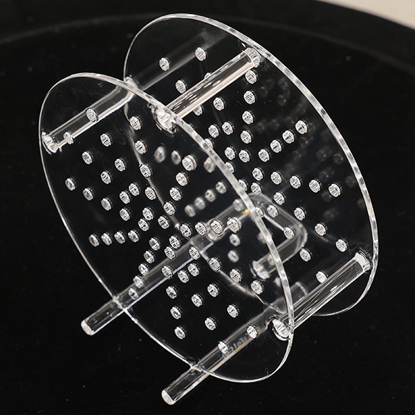
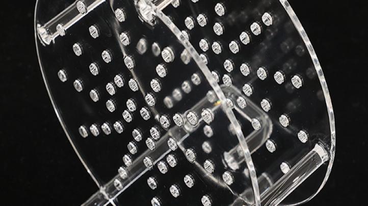
A quartz baffle is a specially designed plate or barrier made from high-purity quartz (typically >99.99% SiO₂), installed within CVD reactors, plasma chambers, or thermal processing equipment. Its purpose is to control gas flow dynamics, improve thermal uniformity, and shield sensitive components from contaminants or radiant heat.
Depending on the system’s design, quartz baffles can be flat, slotted, curved, or perforated, providing full customization to meet the needs of custom quartz fabrication projects.
Quartz Baffle Structure Overview
Material Characteristics
-
Made of fused silica or synthetic quartz, ensuring high thermal resistance, chemical inertness, and excellent optical clarity.
-
Softening point around 1,730°C, ideal for use in LPCVD, PECVD, and RTP systems.
-
Low coefficient of thermal expansion for dimensional stability in fluctuating temperatures.
Structural Forms
-
Flat baffle plates: Common in horizontal furnaces to create laminar gas flow.
-
Perforated baffles: Promote uniform gas distribution across wafers.
-
Ring baffles or tube-shaped baffles: Used to isolate or redirect plasma streams in etching systems.
-
Optional features include slots, tabs, or support notches for integration with quartz wafer carriers or jigs.
Functions of a Quartz Baffle in Semiconductor Processing
Gas Flow Management
Quartz baffles are primarily used to regulate gas flow inside process chambers. In chemical vapor deposition (CVD) systems, precise gas dispersion ensures uniform thin-film formation on silicon wafers. A well-placed baffle minimizes turbulence and backflow, creating more consistent reaction zones.
Thermal Uniformity Control
By acting as a thermal shield or deflector, the baffle helps prevent localized overheating. This contributes to a more stable thermal profile across the wafer batch, which is critical for process repeatability in semiconductor fabrication.
Particle Contamination Reduction
In high-purity environments, even microscopic contamination can destroy an entire lot. Quartz baffles act as physical barriers to stop particles—whether from tooling, reaction byproducts, or chamber walls—from reaching the wafers.
Plasma Shielding
In plasma-enhanced processes such as PECVD or plasma etching, quartz baffles can shield certain areas from direct ion bombardment. This selective exposure allows for more precise etching patterns or deposition layers.
Why Choose High-Purity Quartz Baffles?
Using baffles made from semiconductor-grade quartzware ensures:
-
High-temperature resilience in prolonged processing cycles
-
Chemical resistance to corrosive gases like HCl, NF₃, or O₃
-
Minimal outgassing or particle shedding
-
Longer lifecycle compared to ceramic or metal alternatives
Applications of Quartz Baffle Across Industries
| Industry | Application |
| Semiconductor | LPCVD/PECVD process chambers, wafer diffusion |
| Photovoltaic | Solar cell coating lines, gas flow homogenization |
| LED/OLED | Thin film deposition chambers |
| Optics | High-vacuum thermal treatment systems |
| Research Labs | Plasma research setups, cleanroom process chambers |
Though often overlooked, the quartz baffle is a silent workhorse in high-precision processing. Whether you're optimizing for gas flow control, thermal stability, or contamination prevention, choosing the right baffle design and material can significantly enhance process outcomes.
If you're sourcing high-purity custom quartz components for your semiconductor or photovoltaic systems, be sure to work with manufacturers who understand the intricate roles these small but mighty parts play. Feel free to contact DKEQ!